- Processing line for perovskite modules up to 35x35 cm2
- Psk/Si tandem processing tools
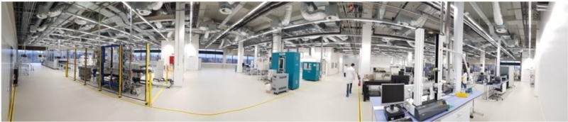
- Characterization and stability testing equipment
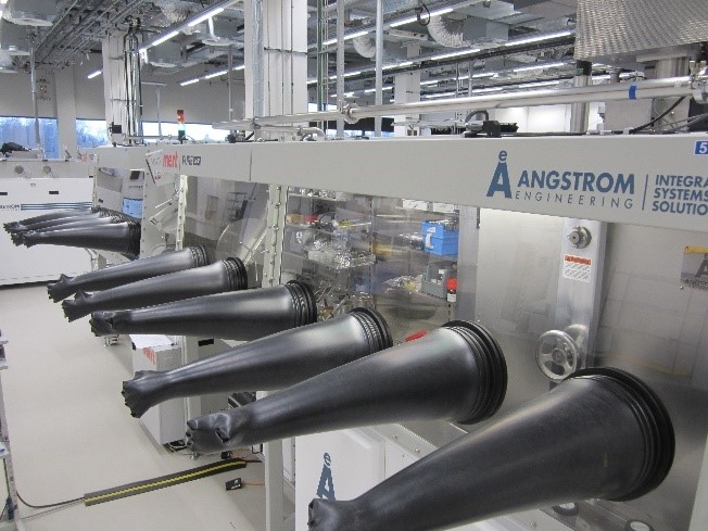
IMEC perovskite assembly line allows to process full modules up to 35x35cm². A slot die coater can deposit solution-based materials while a vacuum thermal evaporation, with 4 sources, and sputtering system, with RF and DC targets, makes a combination of oxide and metallic coatings accessible for both passivation and electrode layers. IMEC developed soft sputtering processes for metal oxides atop perovskite stack without causing damage to the underneath fragile layer stack. In addition, a versatile 3-wavelength picosecond laser system is available for the creation of very narrow interconnections between adjacent cells in the modules. Dispenser, curing stations are available to complete the module packaging. All of these tools are integrated in or connected to controlled atmosphere gloveboxes. A double membrane laminator and screen-printers for patterned metal contacts are also availabe in ambient atmosphere. This enables to create opaque or semi-transparent modules, either rigid or flexible.
Several material and device characterization techniques are available, ranging from scanning electron microscope, Dektak profilometer and 3D confocal microscope, time-resolved photoluminescence, UV-Vis absorbance-reflection measurements, Hall effect, sheet resistance, electroluminescence imaging and high-resolution spectral response to climate chambers for damp heat, thermal cycling and UV testing.
Several class A solar simulators, in ambient as well as in inert atmosphere, are operational for small area devices up to 10x10cm2 modules. Characterization of the large area modules can be done with a large-area LED-light-based solar simulator which can provide A+A+A+ light quality over 1x1.6m2 area and also integrated back lighting for bifacial modules. Electroluminescence measurement of full-size modules with a resolution of <150 um is also possible in the same setup.
| Infrastructure short video presentation here | ||||
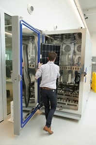
Photo

Description of the infrastructure
IMEC Perovskite assembly line allows to process full perovskite modules up to 35x35cm² as well as Pk/Si tandem of full wafer size.
The line allows versatility of carrier materials to be used, ranging from glass, plastic to metal sheets. This enables to create opaque or semi-transparent modules, either rigid or flexible. Variable interconnection schemes can be developed with the laser system to fabricate customised modules.
• Customised solar modules
• opaque or semi-transparent modules, either rigid or flexible
• Tandem solar cells
• IoT up to BIPV
A slot die coater can deposit solution-based materials while a vacuum thermal evaporation, with 4 sources, and sputtering system, with RF and DC targets, makes a combination of oxide and metallic coatings accessible for both passivation and electrode layers.
IMEC developed soft sputtering processes for metal oxides atop perovskite stack without causing damage to the underneath fragile layer stack.
In addition, a versatile 3-wavelength picosecond laser system is available for the creation of very narrow interconnections between adjacent cells in the modules. Dispenser and curing stations are available to complete the module packaging.
All of these tools are integrated in or connected to controlled atmosphere gloveboxes.
A double membrane laminator and screen-printers for patterned metal contacts are also availabe in ambient atmosphere. Additionally, material and device architecture evaluation are possible on small area devices (<1cm²) up to minimodules (10x10cm²) with versatile tools like spin coaters, vacuum thermal evaporation and sputter systems, and mechanical scriber suitable for such smaller area devices.
Several material and device characterization techniques are available, ranging from
- scanning electron microscope,
- Dektak profilometer and 3D confocal microscope,
- time-resolved photoluminescence,
- UV-Vis absorbance-reflection measurements,
- electroluminescence imaging
- high-resolution spectral response
- climate chambers for damp heat,
- thermal cycling and UV testing.
Several class A solar simulators, in ambient as well as in inert atmosphere, are operational for small area devices up to 10x10cm2 modules.
Characterization of the large area modules can be done with a large-area LED-light-based solar simulator which can provide A+A+A+ light quality over 1x1.6m2 area and also integrated back lighting for bifacial modules. Electroluminescence measurement of full-size modules with a resolution of
Services currently offered by the infrastructure
The Thin-Film Photovoltaic Lab of IMEC is open for use by all our (industrial) partners with whom we have a collaboration agreement. Industrial residents that stay for a longer period at IMEC can get a training on the tools and get direct access to operate the tools themselves. For occasional visitors wanting to execute experiments, our scientific and technical staff are operating the tools. We have state-of-the-art and stable processes in place guaranteeing that high-quality research can be performed in these facilities. As a very recent example of this we can refer to the perovskite on CIGS tandem device with an efficiency > 25% that recently was made in our infrastructure with the collaboration of many international partners: https://www.pv-magazine.com/2020/02/27/international-consortium-claims-25-efficiency-for-flexible-cigs-solar-cell/.
In the last two years we had many users from companies and institutes from outside Belgium using our facilities (e.g. from France, Japan, Germany, ...).
Modality of access under this proposal
- Details on access: Desk and PC availability, support for arranging accommodation, introductory and safety trainings to allow lab access
- Number of days spent typically at the infrastructure for an experiment: 5 -10 days, to follow all steps of full experimental run; a short training in the lab for entering the facilities and for the safety will be always supplied with support of assistants; to carry out independently experiments more intense lab and tool training is required, consequently a longer stay should be foreseen
- Unit of access (how many user visits are expected): 5 users per year; before any access, preparatory planning by telco and/or exchanges of information is to be included, as well as afterwards joint data analysis (by email) and conclusions (by telco) are to be counted
- Remarks on integration of users into the scheduling of the RI: IMEC in agreement with the user will plan the visit and use of tools at the facility, whereby the scheduling will be in accordance with the priority needs of IMEC
- Access costs: combination of unit costs and actual costs, as it depends on the type of equipment to be used and the need to fully dedicate its use to the visit or shared use with IMEC team members can be arranged
Support offered under this proposal
For the thin-film PV activities, a team of 5 experienced researchers, together with another 5 PhD students, are available to advise and operate activities from materials research up to module processing. Another team of 3 trained technicians can also further assist in the experiments. Relocation support is offered by IMEC’s HR services.
Partecipation in others relevant Research Projects or activities connected to VIPERLAB
The IMEC Thin-Film PV Technology team has been involved in several H2020 projects on organic (Mujulima, ArtESun) and perovskite (ESPResSO) solar cell technology. Also national funded projects (PVme, PROMISES) in those fields have been concluded successfully. It is currently also involved in H2020 project PERCISTAND, on perovskite/CIS tandems, and the infrastructure project VIPERLAB.
Expertise
Infrastructure's main contact

VIPERLAB Infrastructure's contact

Other Expert