- Sheet-to-sheet process line for perovskite solar cells and modules (6x6 inch2) based on industrial compatible processes (slot die, xALD, sputter, laser interconnect, encapsulation
- The infrastructure can be used to manufacture rigid, flexible and opaque or semi-transparent (or translucent) modules
TNO is partner in Solliance a Dutch, Flemish, German partnership that wants to realize a concentration of effort of the parties involved in research in the manufacture, installation and use of systems for energy generation by solar cells.
TNO possesses a research infrastructure enabling the complete process of perovskite modules on an area up to 6-inch squares. Thereby many industrial and academic partners in the Solliance consortium have access to this infrastructure with the capability of making efficient and stable perovskite modules on large area, As example:
New material can be tested with scalable process on cell and module level and the loss of upscaling can be analysed as the area of device increases by about 4 orders magnitude; from the size of typical lab cells (in the order of square millimetres) to 6-inch modules.
Besides these material and device processing aspects, the infrastructure can also be utilized to manufacture a set of nearly identical perovskite modules to support other research purposes, e.g. outdoor testing, demonstrators, prototypes, tandem devices, etc.
In addition, next to rigid substrates, the line can also handle flexible substrates and can thus be utilized to process flexible perovskite modules. Figure 1 shows the pictures of perovskite cells and modules processed on rigid and flexible substrates.

Figure 1 pictures of various devices: a) small cells processed on 6-inch substrate, b) semi-transparent rigid module, c) opaque flex module
One important application of perovskite solar cells is to form tandem devices with some commercialized PV technologies such as Si and CIGS. At TNO there is know-how for making perovskite cells directly on silicon wafers and devices with extremely high near-infrared transparency. This enables the manufacturing of two terminal and four terminal devices. This infrastructure can facilitate the tests of new materials and device architectures with reproducible and scalable processes and thereby the perovskite PV technologies can be investigated in both large-area modules and common small lab cells with good statistics.
In the past within the Solliance consortium, many partners brought their materials such as polymer, metal oxide, TCO and encapsulants, to test them in the perovskite devices processed using this infrastructure. TNO also provided perovskite devices to different institutes to develop new characterization and modelling techniques. Within the Solliance research community the international users use the TNO infrastructure approximately once a month and there are also commercial partners and partners outside Solliance who use it about 3 times a year
Services currently offered by the infrastructure
The key equipment includes:
- sputter tools for depositing transparent conductive oxide (TCO),
- sheet-to-sheet (S2S)
- slot-die coaters under inert and ambient conditions for perovskite and carrier transport layers (CTLs),
- S2S spatial atomic layer deposition (sALD)
- tools for CTLs and buffer layers,
- S2S laser interconnection tools with safe processing of toxic materials,
- S2S glass/glass or glass/thin film barrier encapsulation tools.
With respect to each equipment, reproducible material processes have been developed in order to fabricate efficient and stable perovskite modules.
So far the 6 inch perovskite modules processed at the infrastructure of TNO shows an aperture-area efficiency of 13~14.5% in a semi-transparent configuration and 15~16% in an opaque configuration.
Furthermore, the encapsulated perovskite modules can retain over 90% of their initial performance after over 1000 hours of light soaking, damp heat and thermal cycling tests respectively.
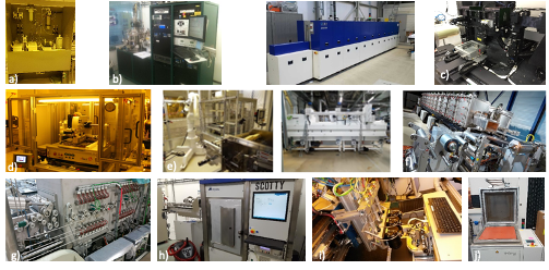
Figure 2 pictures of equipment for the complete process of 6 inch perovskite module: a) Glass cleaning facility, b) two sputter tools for TCO and metal , c) laser system for scribing, d) S2S slot-die coater, e) automated S2S coating system with slot-die coater and oven, f) roll-to-roll slot-die coater and oven, g) spatial ALD, h) e-beam evaporator, i) ink-jet printer and j) encapsulation tool
To access under VIPERLAB Project
- Details on access: about 42 days per year can be offered to external users. This is based on 5 experiments during the project duration of 42 months. An experiment takes approximately 6 weeks.)
- Number of days spent typically at the infrastructure for an experiment: depending on the availability of equipment and operators, the time of one experiment (from substrate preparation to module encapsulation followed by various characterizations) could last 6 weeks.
- Unit of access (how many user visits are expected): approximately 1-2 users a year.
- Remarks on integration of users into the scheduling of the RI: A complete experimental cycle includes several phases. The first phase covers the planning of the experiment. This includes planning operators and equipment and ordering materials and disposables. The second phase is the execution phase where the samples are prepared from substrate to encapsulated device. In the third phase, the devices are characterized. Typically, the second phase is to be carried out by experienced TNO staff. The users can visit the facility where the processes can be explained.
Access costs: a calculation is made according to the actual access cost method. This gives a calculated cost of 106.810 EUR for 5 experiments during the project period. So, the access cost for a single experiment is calculated to be ∼21.360 EUR
Support offered
For trans-national access, the users could come to Eindhoven in the Netherlands where the infrastructure is located. The module processing and the following characterization and analysis usually take several weeks. The experimental plan will be agreed on after the discussion between the users and TNO staffs. A complete experimental cycle can take six weeks. The cycle includes several phases. The first phase covers the planning of the experiment. This includes planning operators and equipment and ordering materials and disposable. The second phase is the execution phase where the samples are prepared from substrate to encapsulated device. In the third phase, the devices are characterized. Typically, the second phase is to be carried out by experienced TNO staff. The users can visit the facility where the processes can be explained.
For virtual access, if the users want to test their new materials in the perovskite modules, they can ship their materials to TNO and then the modules will be processed, characterized and analysed. The users will receive a report about the results. In case new materials, are evaluated in the S2S process, preliminary tests will be required to determine compatibility with the perovskite device stack, scalable process methods, process conditions and offered equipment.
If users need perovskite cells or modules for reliability, characterization or modelling studies, the devices can be fabricated and shipped to the users for more in-depth characterization or analysis
Participation in Research project
The infrastructure is participating in several national and international research and industrial projects in
- Experimental studies and prototyping on different single junction and hybrid tandem cell types and designs
- Flexible and rigid perovskite single junction cells and modules
- Top cell or module of mono and bifacial hybrid tandems
Particularly:
- HiperXL – Solar-era.net project for the development of bifacial hybrid tandems
- NanoQI - targets industry-suited, real-time and in-line capable technique to characterise nano-structure and nano-dimensions
- H2020-VIPERLAB
Expertise
VIPERLAB Infrastructure's contact

VIPERLAB Infrastructure's staff