Solar cell manufacturing & characterization
- High efficiency silicon bottom cells
- Vacuum and wet chemical processing of layers for perovskite tandem solar cells
- Metallisation concepts
- Electrical and optical analyses of perovskite silicon tandem cells and precursers
- High resolution analyses down to the nano scale
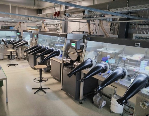
Fraunhofer will provide silicon bottom solar cells, and infrastructure for solar cell processing, including a range of vacuum deposition technologies, wet-chemical perovskite processing, metallisation and interconnection technology. Baseline processes are available that allow for high efficiencies. Furthermore, characterization equipment will be available for electrical and optical analysis of perovskite and perovskite-silicon tandem cells and precursors, as well as micro- and nano-analytics for root cause analysis (see description infrastructure).
Photo

Description
Solar Cell Manufacturing
- High efficiency silicon (HTJ, TOPCon) bottom solar cells
- Range of vacuum deposition technologies: TCO and selective contact sputtering, evaporation (metal, organics, metal oxides), ALD (SnOx, AlOx, ZTO ...).
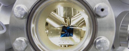
- Vacuum deposition of perovskite absorbers (currently 3 independent sources, upgraded to 5 independent sources under way), also hybrid processing with subsequent wet-chemical processing.
- Wet chemical processing of perovskite solar cells (spin coating, spray coating, blade coating, inkjet) in glovebox setups.
- Perovskite silicon tandem solar cell base lines, currently efficiencies of n-i-p 23.4 %, and p-i-n 25.1 %
- Range of metallisation concepts (evaporation, screen printing, dispense, plating ...)
- Electrically conductive adhesive bonding for low-T interconnection for later module incorporation
- Fabrication of specific test structures and devices (laser processing, soldering, lamination/encapsulation) (Halle)
- Processing is possible throughout for sample sizes of up to 156x156 mm2.
Characterisation:
- Various sun simulators with continuous illumination source and adjustable spectrum (LED-Solar) and irradiance, optimized for the analysis of perovskite and perovskite tandem solar cells
- External Quantum Efficiency (EQE) Setups, optimized for different applications, e.g. tandem solar cells, larger areas, including appropriate bias light sources
- Fully integrated solar cell characterization tool, including IV, EQE, Reflection, Light Beam Induced Current (LBIC) for Quantum Efficiency (QE) maps with multiple color excitation
- Camera-based luminescence imaging analysis is provided including monochromatic and spatially homogeneous laser illumination at two different wavelengths (532 nm and 790 nm) and a high-end silicon camera sensitive in the VIS-1100nm wavelength range. A defined voltage can be applied for electroluminescence imaging or combined measurements. Cells of up to approx. 160x160 mm² can be measured.
- Camera-based lock-in thermography enabling spatially resolved power dissipation analysis is provided. LED-based illumination at different wavelengths (470 nm, 655 nm, 950 nm) can be used for carrier excitation at different sub-cells. Alternatively, or in combination with illumination, a defined voltage can be applied. Lock-in based measurements enable the detection of smallest temperature differences resulting from localised power dissipation. Devices of up to approx. 200x200 mm² can be measured.
- Microscopic photoluminescence spectroscopy via confocal microscopy with various excitation wavelengths (532 nm, 640 nm, 905 nm) and high spatial resolution (approx. 1µm).
- Defect localization at module level (EL, LIT, EQE, PL, Raman, Microscopy, X-ray tomography) (Halle)
- Target preparation (metallography, fs/ps/ns-laser preparation, FIB techniques) (Halle)
- LED SoSim & High Resolution Hyper Spectral Imaging (Halle)
- Micro analysis (SEM/EDS/EBSD/EBIC, µLBIC, electrical and optical micro characterization, ICPMS, LIBS) (Halle)
- High resolution nano-analytics (TEM, TOFSIMS, XPS/UPS, AES, ISS) (Halle
Services currently offered by the infrastructure
Solar Cell Manufacturing
- Silicon bottom solar cells or precursor structure with varying surface textures e.g. planar, random pyramids, are made available to groups seeking to test their perovskite technologies in the context of perovskite silicon tandem solar cells.
- Deposition of layers or layer stacks is offered to complement existing perovskite manufacturing to realize complete devices and/or benchmark own processes. Although the development and optimization of specific process routines and recipes is offered.
- Vacuum and hybrid deposition of perovskite absorbers is offered for testing specific perovskite compositions and/or achieving conformal coating of textured substrates.
- Wet chemical processing of perovskite absorbers and contact layer is offered for testing specific perovskite compositions and contact materials.
- High-efficiency, low-temperature baseline processes are available for both n-i-p and p-i-n silicon tandem solar cells as benchmark and testing environment, e.g. for new absorber and/or contact materials.
- Metallisation of different kind of solar cells is offered, varying in size and also intended TRL level and potential for upscaling.
- Interconnection of sub-cells with temperature sensitivity in strings to demonstrate larger modules is offered.
Characterisation:
- State-of-the art characterisation of perovskite and perovskite on silicon solar cells is offered. These analyses comprise global measurements, and camera-based measurements, which enable measurements of the whole cell area up to microscopic measurements with highest resolution. Offered services are
- IV-measurements with setups including an adjustable spectrum and measurement protocols suitable for metastable cells.
- EQE measurements on perovskite and perovskite tandem solar cells. Usage of the integrated setup allows for fast acquisition of IV, EQE, Reflection, and LBIC for single junction solar cells.
Spatially resolved luminescence imaging, lock-in thermography and light beam induced current maps are used for identifying spatial inhomogeneities. For example, voltage dependent power dissipation in a perovskite solar cell measured by dark lock-in thermography revealing areas of increased recombination / areas of decreased parallel resistance. The combination of LBIC, photoluminescence and thermography is used for a fully integrated solar cell characterisation, allowing for the quantification of non-homogenous losses of perovskite solar cells, as depicted in fig. 1
Fig. 1 Example of spatially resolved assessment of cell parameters short circuit current, open circuit voltage and efficicency of a (blade coated) perovskite solar cell. Inhomogeneous losses can be quantified in order to give advice for further device optimisation. ( Mundt, L. E., Kwapil, W., Yakoob, M. A., Herterich, J. P., Kohlstädt, M., Würfel, U., ... & Glunz, S. W. (2019). Quantitative Local Loss Analysis of Blade-Coated Perovskite Solar Cells. IEEE Journal of Photovoltaics, 9(2), 452-459.
- Micro photoluminescence spectroscopy is used for the selective analyses of top cell and bottom cell via wavelength dependent excitation, while time dependent PL analyses enable analysing the recombination properties of excited layers (perovskite, silicon)
- Root cause analysis by defect diagnostics on the micro- and nanoscale.
Only combining the different methodologies ranging from global measurements to nano-scale root cause analysis allows for a holistic understanding and access at different locations is therefore offered as one infrastructure.
Services are currently offered either by short and long term R&D contracts, as well as by receiving guest scientist. Currently > 60 (>50 (Halle)) external guests/year (international students, PhD and scientific exchange) are using the different facilities
To access under VIPERLAB Project
Access can be granted on the basis of evaluated proposals which describe the envisaged experiments of a user. Typical times of using this infrastructure is between 1 week (measurement on existing samples) and 4 weeks (processing and characterization) depending on the type of experiments. An expert from Fraunhofer will offer guidance for these measurements including safety and detailed technical training and will accompany the experiments.
Support offered
Services offered include the guided access to the above described characterisation techniques. Together with a Fraunhofer ISE/CSP - expert experiments can be performed, data can be evaluated, and conclusions can be drawn.
Partecipation in others relevant Research Projects or activities connected to VIPERLAB
Contact the infrastucture
Expertise