ENEA has been developing over the past few decades a strong expertise on photovoltaic devices starting from thin-film and crystalline silicon based solar cells to last generation of organic/hybrid materials for PV. At the present, the proposed infrastructure is mainly devoted to the fabrication and characterization of perovskite solar cells to be used in 2T monolithic perovskite/silicon tandem solar cells.
The infrastructure comprises (main equipment):
- Three glove boxes (one in nitrogen atmosphere, one in nitrogen or dry air atmosphere with controlled relative humidity in the range of 5 % - 70 %, and one equipped with a thermal evaporator for electric contacts);
- PECVD (standard and VHF) multichambered for doped and intrinsic silicon-based thin films (maximum area 4” or 10 x 10 cm2);
- Radio-frequency magnetron sputtering for AZO and ITO deposition (maximum area 30 x 30 cm2);
- Electron-beam and thermal evaporation systems used for MgF2, ZnS, LiF, MoOx and metals;
- Several ovens for conventional and RT thermal processes in a wide range
- UV-ozone treatment;
- Material characterization techniques (Raman microscopy, UV/Vis/NIR spectrometry, photoluminescence, ellipsometry, SEM/EDX, FIB, AFM, 4-point probe resistivity, Kelvin probe, photoconductance decay technique, Impedance spectroscopy);
- Tools for solar cells fabrication and innovative modules realization has been acquired (installation: October 2020, availability to access: March 2021)
- Multi-source thermal evaporation system for perovskites (maximum area 4” or 10 x 10 cm2)
- larger area PECVD system specifically developed for high-efficiency silicon heterojunction solar cells able to process 4 wafers (6”) at the same time
Solar simulator with sensitivity to a broader range of wavelengths, at least between 300 nm and 1200 nm, and with longer lamp pulse duration, at least 100 ms or steady state, to characterize innovative PV materials and with the possibility of heating the samples for determining the temperature coefficients and for energy rating estimation
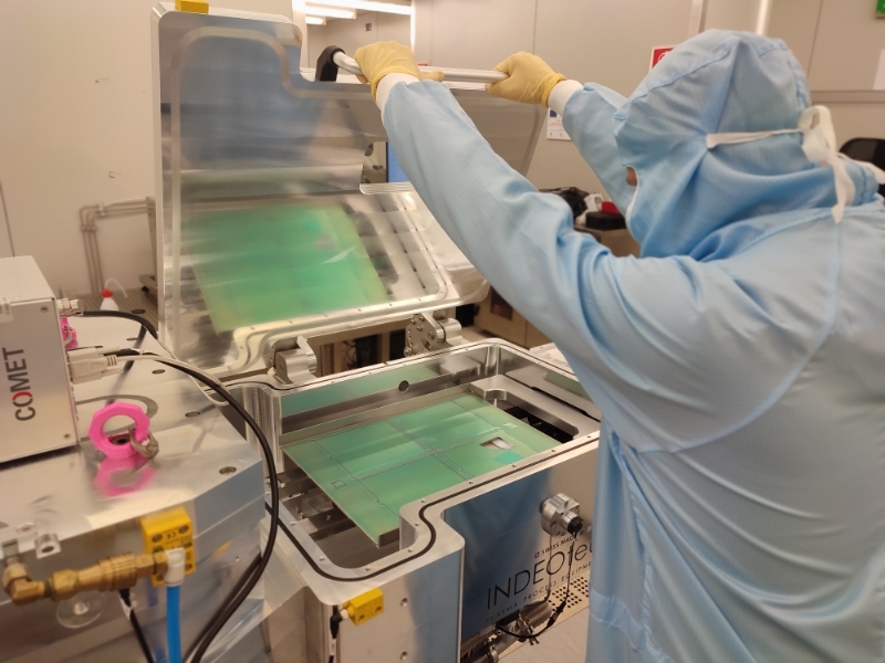
Photo
test
extra test
Lab's Equipment & Instruments
