The infrastructure offer access to:
- Perovskite/silicon tandem processing
- Vapor deposition of contacts, electrodes and perovskite precursors
- Tandem characterization
The joint Swiss Center for Electronics and Microtechnology (CSEM) and the École polytechnique fédérale de Lausanne (EPFL) Research Infrastructure for the PV Perovskite is focussed on R&D efforts to improve efficiency and stability of PSK/Si Solar cells to allow their scaling up onto larger surface
This laboratory claims to have overcome in July 2022 the conversion efficiency exceeding 30% for a 1 cm2 tandem perovskite-silicon solar cell, which represents the first time of a world record for a PV device of this kind. In particular it has been obtained an efficiency of 30.93% for a 1 cm2 solar cell based on high-quality perovskite layers from solution on a planarized silicon surface and 31.25% on a 1 cm2 solar cells fabricated with a hybrid vapor/solution processing technique compatible with a textured silicon surface.
Both efficiencies were indipentently certified by the US Department of Energy's National Renewable Energy Laboratory (NREL).
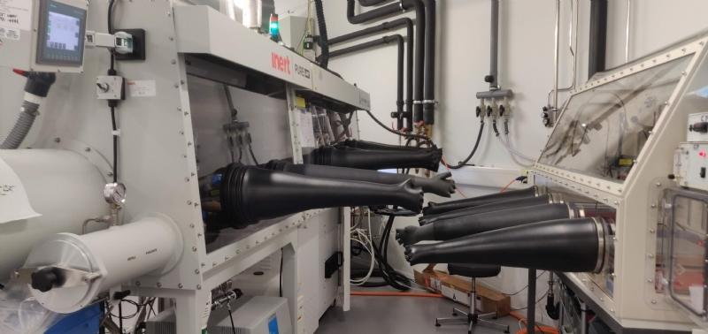
Photo
Description of the infrastucture
EPFL-PVLAB and CSEM-PVcenter share perovskite deposition facilities, which aim at developing high-efficiency PSK/Si tandem solar cells. Access will be offered to the following equipment:
- A multi-source evaporator for the deposition of inorganic perovskites or its inorganic precursors, compatible with flat and textured Si wafers (up to 6 inches).
- A multi-source magnetron sputtering tool for the deposition of charge carrier-selective contacts, transparent conductive oxides and metal electrodes (ITO, IWO, NiO, MoOx, SnOx, Ag, etc.).
- An atomic layer deposition system for buffer layer deposition (SnOx, AlOx).
- Metrology tools for perovskite (tandem) characterisation, including a 2-lamp (Xe, Ha) class AAA sun simulator, external quantum efficiency measurement setup with electrical and light bias for multi-junction measurement, photothermal deflection spectroscopy, microscope-based photoluminescence and Raman spectroscopy, spectroscopic ellipsometry.
Services currently offered by the infrastructure
The infrastructure serves mainly members of both institutes and enables to process perovskite/c-Si tandems from initial c-Si wafers up until the final thin-film layers of the device and its characterisation. This infrastructure has enabled EPFL PVLAB and CSEM PVcenter to play a key role in the field of perovskite/c-Si tandems, notably by demonstrating the first tandems surpassing an efficiency of 25 % (with a fully textured design) or full-area 4-inch tandems with an efficiency above 24%. Some of the small-scale devices reaching these efficiencies also featured c-Si bottom cells textured on both sides for optimal light management, a world first. The concept was then pushed one-step further by demonstrating the first perovskite on silicon triple-junction solar cell. External users now mostly come to access metrology tools, with processing systems mainly accessed by internal users.
Modality of access under VIPERLAB Project
- Location: perovskite processing facility at EPFL Neuchâtel, Switzerland
- Details on access: EPFL & CSEM will offer 45 days for access to external users distributed over the full project duration. Each day of access will cost 2000 € (excluding overheads).
- Number of days spent typically at the infrastructure for an experiment will range from 1 (metrology, single layer processing) to 5 (tandem processing & characterisation)
- Unit of access (how many user visits are expected): Up to 15 days a year, total of 45 days for the full duration of the project.
- Prior to any access, external users will communicate and discuss their experimental plans with the internal staff. Internal staff will make preliminary experiments to assess the viability of the experiments envisaged. Only then will the experimental plan be validated.
- At the facility, external users will be trained to safety and lab practise measures and constantly supervised by staff of the facility. Simple manipulations will be performed by the external user, while more complex ones will be performed by internal staff.
Support offered under this proposal
External users will benefit from the expertise of PVLAB and PVcenter in designing, processing and characterising high-efficiency multi-junction devices. Help with respect to experiments and stack design will include the use of in-house optical simulation tools. Processing and characterisation efforts will be focused on the use of the systems described above. Staff members of PVLAB and PVcenter will also support external users to interpret experimental data.
Partecipation in others relevant projects or activities, connected to VIPERLAB
- CHEOPS Achieving low-cost, highly efficient perovskite solar cells, H2020 (Duration: 2016-2019) (CSEM & EPFL)
- INTENT, developing stable perovskite-silicon tandem devices, SFOE (2018-2021) (EPFL)
- EPISODE, designing novel perovskite materials and charge transporting for high efficiency devices, SNSF (2017-2021) (EPFL)
- POWER, High-performance tandem solar cells with improved stability and cost-competitive manufacturing (2018-2021) (EPFL)
- PV2050, Building blocks for the next generation multi-junction solar cells, SNSF NRP70, (2014-2018) (EPFL)
- H2020 EU PEROCUBE (High-Performance Large Area Organic Perovskite devices for lighting, energy and Pervasive Communications). To be started in April 2020 (CSEM)
- SYNERGY (Realizing photovoltaic energy harvesting systems based on tandem solar cells with efficiency beyond that achievable with state-of-the-art industrial single-junction cells), Swiss National Science Foundation project on perovskite-based cell development(CSEM)
- H2020 EU INREP (Towards Indium Free TCOs; 2015-2018) on the development of Indium free transparent electrodes for PV, LEDs and touchscreens.(CSEM)
Expertise
VIPERLAB Infrastructure's contact