Natalia MATICIUC
Postdoc Researcher
Department Solution Processing of Hybrid Materials & Devices
HZB-Helmholtz-Zentrum Berlin
Role in the project : Technical Manager of the Project.- WP11 leader and fully involved in the transnational access organization and management
Short Bio
Dr. Natalia Maticiuc received her bachelor's (2008) and master's (2010) degrees in physics from the State University of Moldova, after which she obtained a PhD in chemistry and materials technology from Tallinn University of Technology (Estonia) in 2015, where she studied chalcogenide thin films for photovoltaic applications in CdTe and kesterite solar cells. Since 2017, Dr. Maticiuc is at Helmholtz-Zentrum Berlin (Germany) focusing on CIGSe absorber surface analysis and implementation of inorganic HTMs in perovskite-CIGSe tandem devices. Since 2021 she is actively involved in coordination of VIPERLAB project.
Publications
Natalia Maticiuc, Eva Unger, Rutger Schlatmann
Francesco Roca, David Casaburi, Antonella De Maria, Massimo Izzi, Vera La Ferrara, Manuela Ferrara, Paola Delli Veneri, Eva Unger, Natalia Maticiuc, Stephan Abermann, Raquel Alemañ, Aldo Di Carlo, Theodoros Dimopoulos, Jens Hauch, Mykhailo Sytnyk, Narges Yaghooni Nia
Webinars

[1] - Took place on Feb, 08th 2022
Modelling, high performance computing and efficient access to data sets based on data reported in the literature and experimental work are important tools to accelerate research in the field of photovoltaic perovskite, and beyond. With this workshop VIPERLAB presents the importance of these topics for materials science technology and how the 4 virtual infrastructures of Viperlab project can support researchers from academy'and industry, with free access to their computing, modeling tools and the available datasets.
[1] - Took place on Nov, 30th 2022
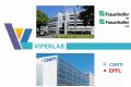
H2020 VIPERLAB Project offers free access to the state-of-the-art perovskite EU infrastructures that cover the whole innovation/value chain from material preparation to characterization of perovskite devices and modules. Today we present two very relevant VIPRLAB research Infastructures: FRAUNHOFER Solar Cell Manufacturing & Characterization & EPFL/CSEM – PV lab/PV Center & PSK/SI Tandem processing.
[1] - Took place on Dec, 15th 2022
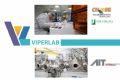
We present other two VIPERLAB Research Infrastructures. The first, CHOSE consists of two main infrastructures: the CHOSE@ROME, is located on the campus of the University of Rome Tor Vergata (Italy), and focuses on technological manufacturing processes and device characterization. CHOSE@TURIN, is an infrastructure associated with the University of Turin (Italy) focused on the development of materials. The secon, AIT Viperlab Reseach infrastructures focusses on characterization and reliability tools for the accreditation tests of PV modules, and tools for PV deposition, characterization/reliability and development of thin film coatings.
[1] - Took place on Jan, 26th 2023
The stability of perovskite devices is a key point should be addressed to achieve commercialisation. The key factors influencing the stability of the devices are the exposure to oxygen and moisture, UV light, solution processing and thermal effects. Encapsulation and standard testing protocols are required to check and improve stability. The two presented infrastructures offer state of the art equipment for the Perovskite Stability testing of materials and devices.
[1] - Took place on Jun, 28th 2023
Perovskite SJ and Pero/Si Tandem technologies are attracting significant attention from both scientific and industrial societies due to rapid increases in efficiency, from approximately 3% in 2009 to over 33% today. Several efforts are made to characterize the technological bottlenecks, overcome them and push the technology to the commercial world through the PV module upscaling. This imposes a pre-industrial stage, where different equipment from coating systems such as blade coating, slot-die coating and spray coating to printing paths such as screen, inkjet and gravure printing as well as methods of vacuum deposition and laser processing are currently used to support the potential of PSCs to move towards their industrialization. VIPERLAB today introduces CEA and IMEC VIPERLAB Research Infrastructures offering State-of-the-art equipment for Fabrication, Characterization, Encapsulation, Upscaling and Testing of Perovskite SJ and Pero/Si Tandem Solar Cells
[1] - Took place on Nov, 13th 2023
Perovskite SJ and Pero/Si Tandem technologies are attracting significant attention from both the scientific and industrial communities thanks to the rapid increases of the conversion efficiency, Several efforts are put on the ground to chracterize the technological bottlenecks, overcome them and to push the technology toward the commercial world through the photovoltaic module upscale. Today we present the TNO-Solliance - S25 Process PSK Line and Swansea University - PV manufacturing and Testing Facilities Research Infrastructure offers state-of-the-art fabrication and characterisation equipment for the printing and testing of solar cells and PV module devices

[1] - Took place on Jan, 11th 2024
The webinar offered by ENEA is devoted to the presentation of the kSEMAW software. kSEMAW is a useful tool for scientists and technicians dealing with optical devices based on optical coatings. More precisely, kSEMAW is a workspace for the analysis of Spectrophotometric (SP), Ellipsometric (ELI) and Photothermal Deflection Spectroscopy (PDS) measurements.
